AD9984A,pdf,datasheet High Performance 10-Bit Display Interfac
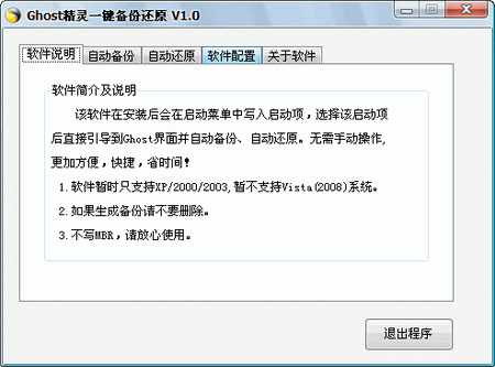
软件大小:345KB
软件语言:简体中文
用户评分:
软件类型:汉化软件
授权方式:免费版
下载官网:www.bblll.com
更新时间:2021-06-06
软件分类:机械电子
运行环境:Vista, Win2003, WinXP, Win2000, NT
杀毒检测
无插件
360通过
腾讯通过
金山通过
The AD9984A is a complete 10-bit, 170 MSPS, monolithic analog interface optimized for capturing YPbPr video and RGB graphics signals. Its 170 MSPS encode rate capability and full power analog bandwidth of 300 MHz support all HDTV video modes up to 1080p, as well as graphics resolutions up to UXGA (1600 × 1200 at 60 Hz).
The AD9984A includes a 170 MHz triple ADC with an internal reference, a PLL, and programmable gain, offset, and clamp control. The user provides only a 1.8 V power supply and an analog input. Three-state CMOS outputs can be powered from 1.8 V to 3.3 V.
The AD9984A on-chip PLL generates a sample clock from the tri-level sync (for YPbPr video) or the horizontal sync (for RGB graphics). Sample clock output frequencies range from 10 MHz to 170 MHz. With internal coast generation, the PLL maintains its output frequency in the absence of a sync input. A 32-step sampling clock phase adjustment is provided. Output data, sync, and clock phase relationships are maintained.
The auto-offset feature can be enabled to automatically restore the signal reference levels and calibrate out any offset differences between the three channels. The auto channel-to-channel gain-matching feature can be enabled to minimize any gain mismatches between the three channels.
The AD9984A also offers full sync processing for composite sync and sync-on-green applications. A clamp signal is generated internally or can be provided by the user through the CLAMP input pin.
Fabricated in an advanced CMOS process, the AD9984A is provided in a space-saving, Pb-free, 80-lead low profile quad flat package (LQFP) or 64-lead lead frame chip scale package (LFCSP) and is specified over the 0°C to 70°C temperature range.
推荐软件
这里推荐一些您可能需要的同类软件下载

2.9M ︱ 简体中文

469KB ︱ 简体中文
AD7823,pdf,datasheet (2.7 V to 5.5 V, 4.5 ms, 8-Bit ADC in 8)
325KB ︱ 简体中文

86.9M ︱ 简体中文

10M ︱ 简体中文

423KB ︱ 简体中文

1.8M ︱ 简体中文
AD7995,pdf,datasheet 4-Channel, 10-Bit ADC with I2C Compatibl
232KB ︱ 简体中文
AD8123,pdf,datasheet Triple Differential Receiver with Adjus
358KB ︱ 简体中文
猜您喜欢
换一换


精品软件推荐


- 下载排行
- 其他推荐
- 1
- 2
- 3
- 4
- 5
- 6
- 7
- 8
- 9
- 10